(China (Mainland))

Product Summary
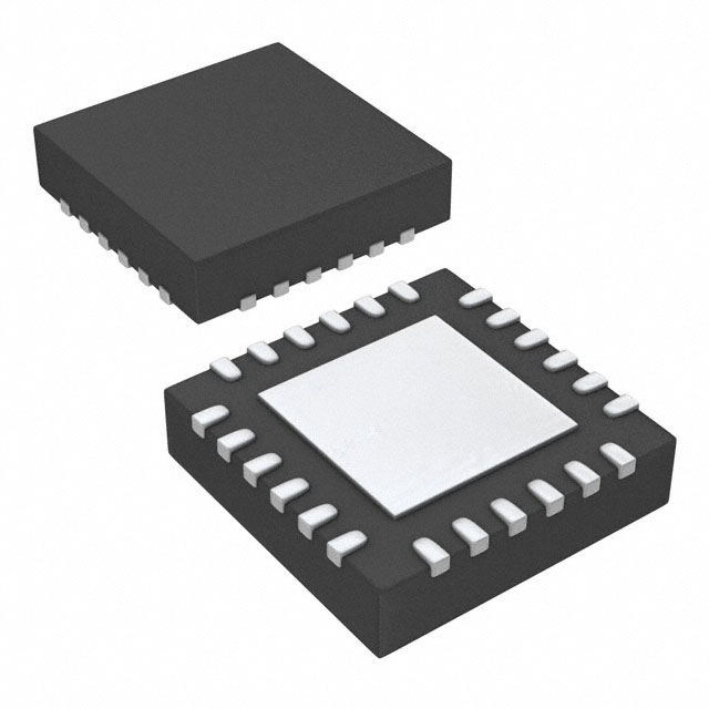
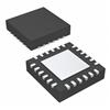
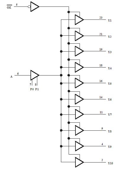
The CDC421250RGET is a high-performance clock-driver circuit that distributes one input (A) to ten outputs (Y) withminimum skew for clock distribution. The output-enable (OE) input disables the outputs to a high-impedancestate. The CDC421250RGET operates at nominal 3.3-V VCC.The propagation delays are adjusted at the factory using the P0 and P1 pins. The factory adjustments ensurethat the part-to-part skew is minimized and is kept within a specified window. Pins P0 and P1 are not intended for customer use and should be connected to GND.
Parametrics
CDC421250RGET absolute maximum ratings: (1)Supply voltage range, VCC:– 0.5 V to 4.6 V; (2)Input voltage range, VI (see Note 1):– 0.5 V to 7 V; (3)Voltage range applied to any output in the high state or power-off state,VO (see Note 1):– 0.5 V to 3.6 V; (4)Current into any output in the low state: IO64 mA; (5)Input clamp current, IIK (VI < 0):–18 mA ; (6)Output clamp current, IOK (VI < 0):– 50 mA; (7)Storage temperature range:– 65 to 150℃.
Features
CDC421250RGET features: (1)Low Output Skew, Low Pulse Skew for Clock-Distribution and Clock-Generation Applications; (2)Operates at 3.3-V VCC; (3)LVTTL-Compatible Inputs and Outputs; (4)Supports Mixed-Mode Signal Operation(5-V Input and Output Voltages With 3.3-VVCC); (5)Distributes One Clock Input to Ten Outputs; (6)Distributed VCC and Ground Pins ReduceSwitching Noise; (7)High-Drive Outputs (–32-mA IOH,32-mA IOL); (8)Significantly Reduces Power Dissipation.
Diagrams
| Image | Part No | Mfg | Description |  |
Pricing (USD) |
Quantity | ||||||||||||
|---|---|---|---|---|---|---|---|---|---|---|---|---|---|---|---|---|---|---|
 |
 CDC421250RGET |
Texas Instruments |
Clock Generators & Support Products Intgr Freq Lo-Jitter Cry Osc Clock Gen |
Data Sheet |
|
|
||||||||||||
 |
CDC421250RGETG4 |
Texas Instruments |
Clock Synthesizer / Jitter Cleaner Fully Int Lo-Jitter Crstal Osc Clock Gen |
Data Sheet |
|
|
||||||||||||